![]()
|
|
Personal web pages ofTim Stinchcombe |
Plan B Model 10 Polyphonic Envelope modificationsIntroduction. The core circuitry within the M10 is a copy of an old (early Seventies) Serge envelope generator, onto which a number of small enhancements and additions have been added by Plan B. Some of the additions don't 'mesh' very well with either the existing circuit or the wider environment in which it is to be used, and it is the 'ironing out' of some of the consequent 'little niggles' with which this page is concerned.
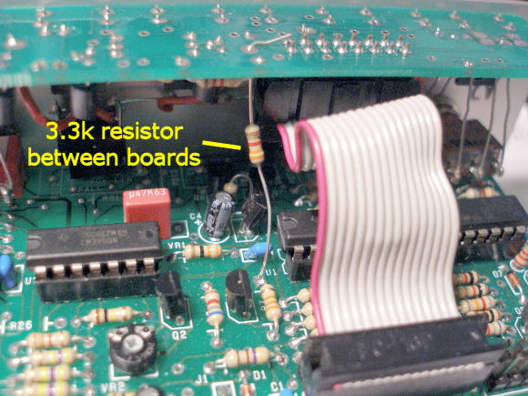
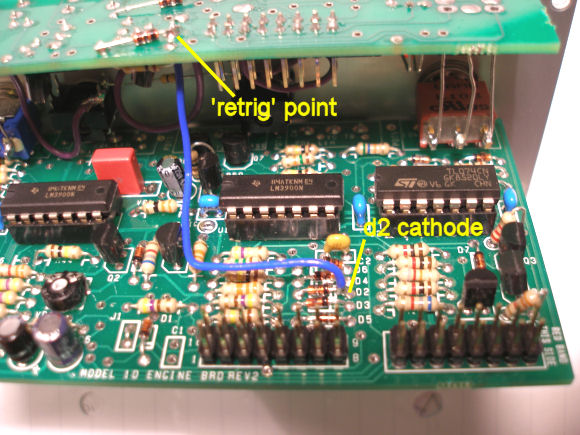
How to identify a module as either a 'MkI' or a 'MkII': the MkII added a 're-trigger' ability to the envelope generator, which forces the envelope to immediately re-start at the beginning if a second trigger pulse is received before the current envelope has completed (so the envelope quickly drops to zero volts, regardless of where it is in its cycle, and then it starts over); the original design will ignore the second trigger, with the envelope having to complete before a new trigger pulse will be recognised. As there is no visual difference in the faceplate due to the re-trigger capability, other than actually trying to re-trigger with the module powered, the only way to identify which mark any particular example is is to spot the differences in the circuitry of the module. The 'rev' level marking in the silkscreen on the main PCB doesn't help here either: the 'rev 2' main board is used in both the MkI and MkII modules; there was a change specific to the MkII version—the addition of a pad for the resistor which runs between the two boards—but this board is also designated Rev 2! (That detail is shown in the photo below) Perhaps the easiest object to spot which shows a module to be an unmodified MkII is this 3.3kΩ resistor running between the two boards:
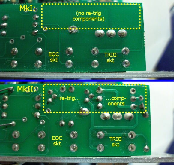
However, this may have been removed and replaced by a wire in one of the modifications below, and so its absence may indicate a modified MkII, in which case a closer look at the components at one end of the smaller 'jack board' will be needed. The re-triggering capability requires the addition of around 9 components, and most of these are situated at the one end of the jack board: absence of these components (at the top of the photo) indicate the module to be a MkI; inclusion of these components show that it is a MkII (bottom):
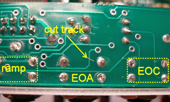
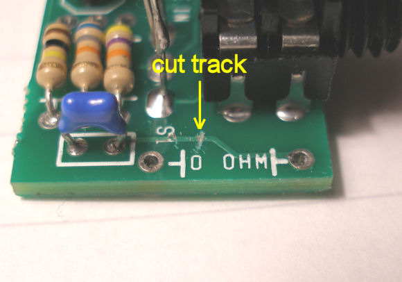
(And unfortunately the last photo doesn't quite show the full story with respect to the MkII board—there are in fact (at least) two MkII jack boards, which have small differences in the region of the re-trigger components. The implications of these differences with respect to the modifications is shown in this photo and the description which follows it.) Protecting diode D4 and preventing voltage out of the 'cycle' input: Diode D4 is probably the most likely one to get damaged, due to the M10's circuit configuration. In 'LFO' mode D4 is basically clamping the 'cycle in' jack to the +12V rail, i.e. about 11.4V appears at the cycle in jack (!). Thus anything inserted into the jack which presents a low impedance path to ground means that virtually the whole 12V rail voltage is imparted across D4, hastening its demise. It is well known for minijacks that inserting a patch cord momentarily shorts the signal pin to ground, so even the simple act of inserting a cord into the cycle in jack whilst in LFO mode may damage D4, especially if the cord is not fully inserted, resulting in a continuous path to ground. The solution is simply to insert another diode between the cycle input and D4—this will be reverse biased under the problem conditions, so preventing any voltage out of the cycle in jack, and is forward biased when a cycle in signal is applied and not in LFO mode. Locate and cut the following track on the jack board:
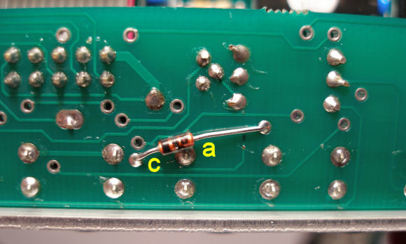
(The annotations refer to the jacks on the other side of the PCB; the MkI and MkII jack board PCBs look to be the same at this spot.) Then solder a 1N4148 (or similar) diode between the vias, anode and cathode oriented as shown; crop the leads short enough to not cause shorts on the component side of the board; and if the body of the diode is placed close to the jack socket pin, there is less chance of it being bent and shorting to that too:
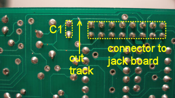
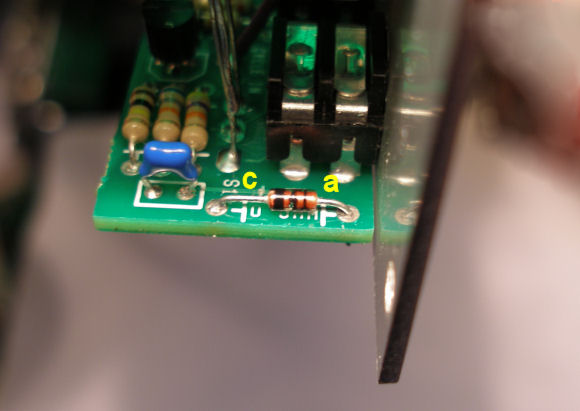
Protecting diodes D1 and D5: D1 and D5 are liable to the same sort of thing, only in this case with respect to the 'trig in' jack, coupled with the gate off the bus (for D1), and the 'start' switch (for D5), and it also requires a more coincidental application of voltage on the bus/switch depressed and the low impedance path to ground appearing at the jack, and thus they are less likely to be damaged (but there are certainly reports of D5 having been blown). The solution is the same—adding another diode (just the one protects both D1 and D5), and the fix is different for MkI and MkII modules (because of the addition of the re-trigger capability on the jack board for the MkII), and unfortunately there are at least two different MkII jack boards in existence, complicating matters further! MkI D1/D5 fix: I think this is best done on the main board (it could be done on the jack board as the MkII fix, but the 'spans' between the useful vias and pins is a bit too great, so would require fiddling around with insulation sleeving etc.). Locate and cut the track under the board joining C1 to the fourth pin in on the ribbon connector:
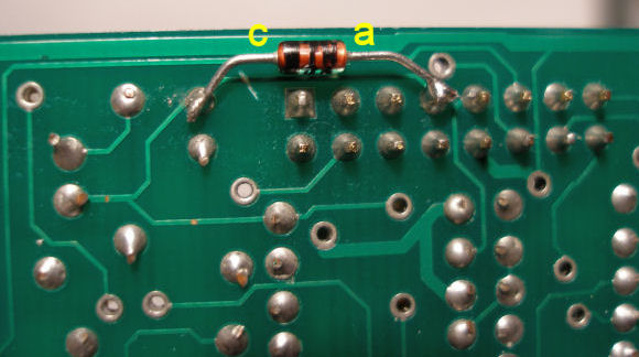
Then solder a 1N4148 diode between these points, oriented as shown, and taking care not to short to anything nearby:
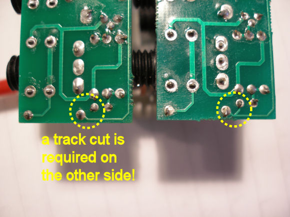
MkII D1/D5 fix: In both cases you need to desolder this zero-ohm link on the jack board (its possible on some boards this may simply be a piece of wire):
Look closely at the solder side underneath this component—you're looking for the short section of track joining the link to the capacitor next to it, or its absence:
If you have the PCB at the left, that connection is made to the other end of the link on the top of the board, and it needs to be cut:
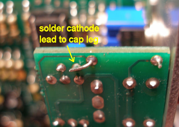
(This is probably best done by removing the jack board from the faceplate, which is not too difficult, but will require desoldering the 're-trigger' resistor linking the two boards.) Then solder in a 1N4148 diode, oriented as shown...
...and bend the cathode lead over and solder to the capacitor leg:
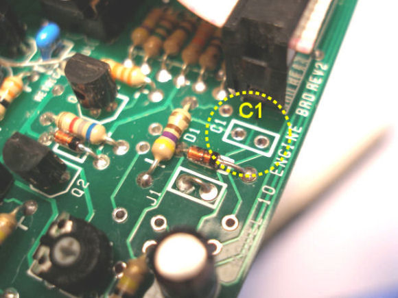
If you have the PCB at right above, there is no track-cutting required, just solder in a 1N4148 (same orientation as photo above), and that is it (no bending over of cathode lead required either!). MkII double-triggering: if you have a MkII M10 which has a 10nF ('103') capacitor installed at C1 (as mine originally had):
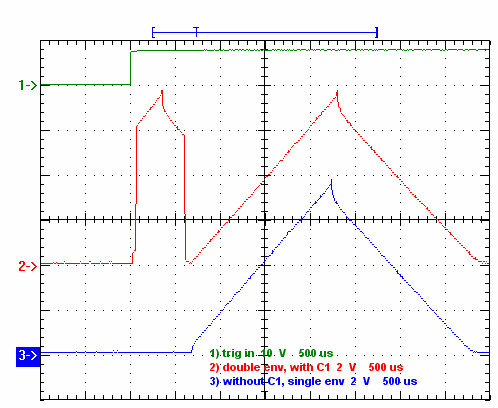
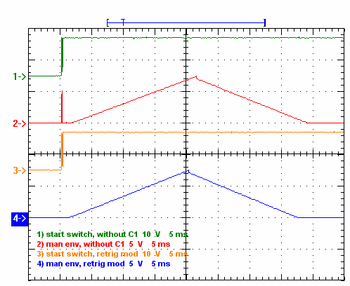
then there is a fair chance that when triggered externally or manually, it 'double-triggers', giving effectively two envelopes out in quick succession, the red trace:
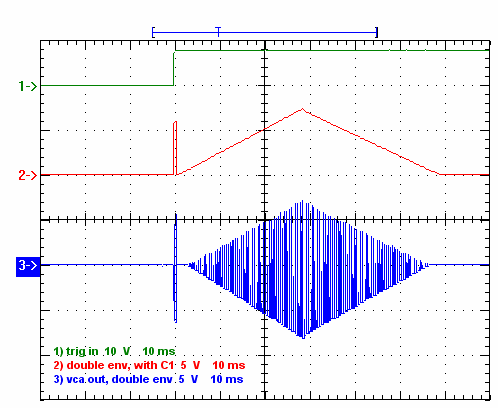
The issue looks worse for quicker envelope settings than for slower ones (note the fast timebase settings in the above plot, chosen to emphasize the problem): the initial spike has a fixed duration, so it looks worse against a short envelope, as then it is a larger proportion of the envelope. The blue trace above also shows how one would really want it to look, and this is simply achieved by removing capacitor C1, and I assume later modules were supplied without that cap fitted, though there is a residual problem discussed further down. It is also quite easy to hear the problem, as this simple sound clip demonstrates: an LFO triggers the M10, in turn controlling an A-132 VCA, which is fed a signal from a VCO; for the middle five repeats in the clip I have switched cap C1 out of the circuit, and the loss of the 'click', caused by the spike, is quite apparent; the following traces show the envelope and the VCA output (to show that the VCA is responding to the fast initial spike; note also this is running much slower than the first set of traces above):
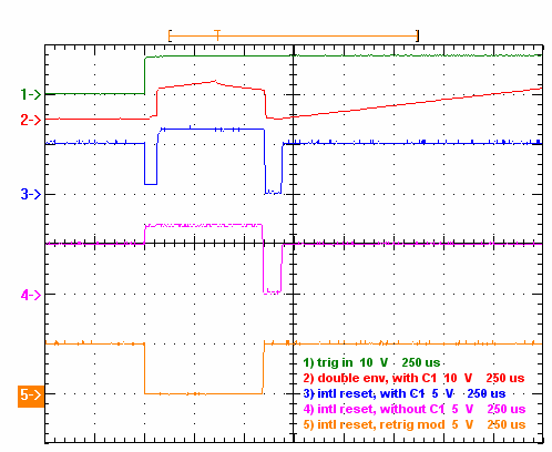
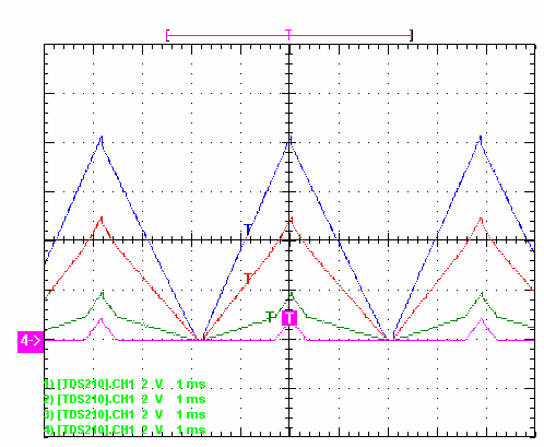
The problem stems from the way the Plan B re-trigger capability interacts with the existing Serge circuitry to reset the main integrator (from whose output the envelope is derived). Before I saw a module that didn't have C1 fitted—which does get around a large part of the problem—I had worked out a modification which appears to sit better with the existing circuit, and which allows re-triggering of envelopes without affecting the normal trigger action. This mod seems to perform better for the small remaining problem when manually triggering the envelope, discussed in a moment, so I have detailed it below as others may want to try it. The internal reset signal is normally high and pulses low to reset the integrator when a trigger arrives. The following set of traces show this signal for the various circuit configurations, along with the originating trigger (green), and the double-envelope (red, and somewhat squashed!) of the problem case for timing-reference purposes:
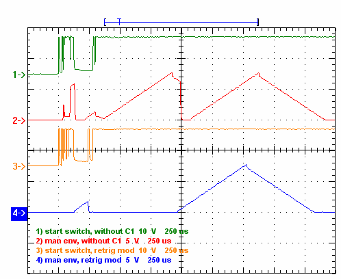
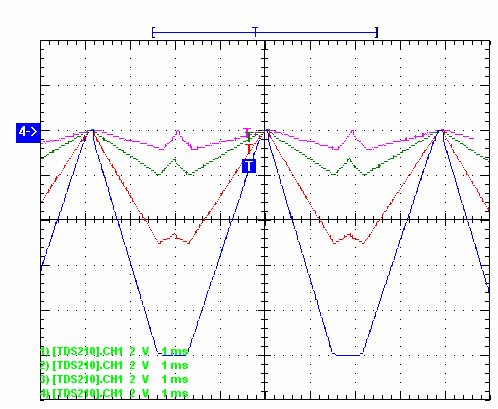
The blue trace is this reset line for an unmodified MkII with C1 in place: the two low pulses are what causes the double-envelope—the first is caused by the 'normal' trigger path through C1; the second is caused by the re-trigger path, due to the addition of the re-trigger circuitry of the MkII module. This also shows another potential issue: the LM3900 chip generating the reset is running off a 6V rail, and the 'high' output is normally sitting at around 5V (i.e. around 1V below the rail, as one would expect) except between the low pulses where the re-trigger circuitry is actually pulling this reset line above 6V, i.e. above the supply rail for the chip—I really have no idea what this might mean for the longer-term health of that chip! The mauve trace shows that removing C1 cuts the straight-through trigger path, and hence the first low pulse is absent, whilst leaving the path through the re-trigger circuit to reset everything with the other low pulse, which it does, hence removing the double-envelope (and again we see the reset pulled greater than 6V). The orange trace is for the mod detailed below—whether C1 is present or not, we get a single low pulse, hence one envelope, and no pulling-up of the chip output above its supply! The residual problem mentioned above is that caused by contact bounce in the 'start' switch, when triggering an envelope manually. Because the MkII is specifically configured to re-trigger, this contact bounce can cause multiple triggering, and (within limits defined by the cap values) corresponding multiple envelopes. The following traces are fairly typical of those obtained from repeated pressing of the 'start' switch: the top pair for a non-modded MkII with no C1; the bottom for the mod given below:
The green and orange traces show the contact bounce well, and for reasons I haven't totally worked out, it is clear that on the whole the mod given below performs better, by not giving as many or as large amplitude envelopes (blue) as the standard MkII configuration gives (red). In fairness to the M10 though I wasn't easily able to generate an audio example which clearly demonstrated aurally that there was any difference between the two (i.e. whilst you can see the spike on a scope, it was hard to actually hear it, so it seems of more academic interest than a practical problem). If we slow down the envelopes, then again in relation to the main envelope, the spike becomes less obvious (and at this timebase I wasn't able to make any little runt spikes appear for the modded version, blue):
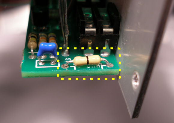
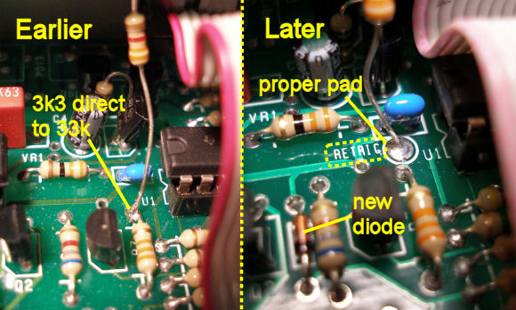
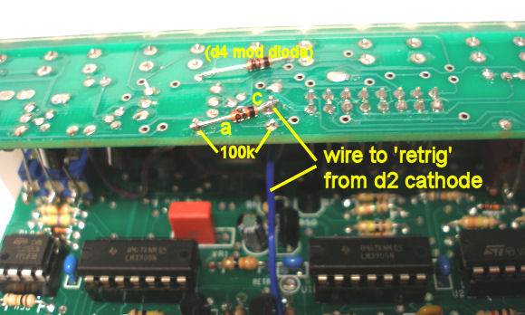
MkII re-trigger mod. Even though there is no impact on the mod, it would be as well to know that there are at least two versions of the main board in existence, both marked 'REV2' (for all I know there could be more):
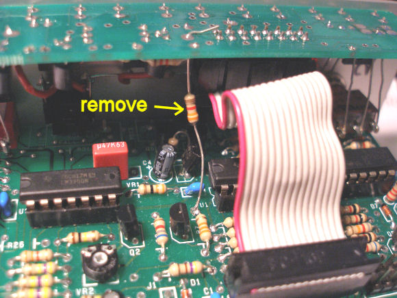
At left, it is clear earlier versions simply had the 3.3kΩ resistor (from the 're-trig' point on the jack board) soldered onto the end of the 33kΩ on the main board; at right, clearly later versions have a proper hole placed on the PCB. Desolder/cut off the 3.3kΩ resistor between the boards:
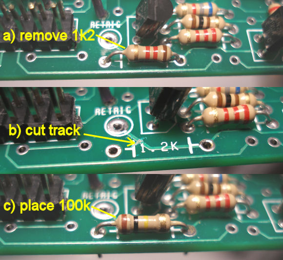
Then remove the ribbon and remove the jack board from the faceplate (just fiddly rather than difficult). After locating this 1.2kΩ resistor on the jack board: remove it; cut the track as shown; solder a 100kΩ resistor in its place:
Re-assemble the jack board and solder a length of wire from D2 cathode to the 're-trig' point on the jack board, leaving the end poking through a bit...
...so that a 1N4148 diode can be soldered between it and the one end of the 100kΩ resistor, in the orientation shown:
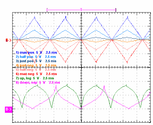
Finally, put the ribbon cable back on! Removing the little 'peaks' in the envelope output: when the 'level' control is set other than fully clockwise, small 'peaks' are evident in the envelope which is output—the following traces are for various 'positive' level-knob settings (in 'LFO' mode):
For 'negative' level-knob settings, the culprit is seen—the blue trace of the fully counter-clockwise setting, i.e. the maximum negative envelope:
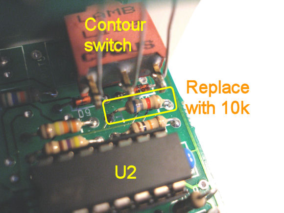
The amplitude of this is clearly several volts more than the maximum positive amplitude (10V cf 8V), causing it to be clipped, and it is this mismatch which causes all the little 'peaks'. They are also readily discernible without using a scope, but with a VCO instead—in this clip the M10 is modulating a VCO, with the level-knob just positive (the M10 is triggered by another LFO), and the quickening of the rate of increase of pitch of the VCO caused by the 'peak' is evident; similarly in this second clip, in which the level-knob is just negative, again the wobble in the pitch is caused by the 'peak' (which actually reverses the direction of the changing pitch). Rectifying this is easy, by swapping one of the gain-setting resistors for the envelope-inverting circuit—change this 6.8kΩ resistor for a 10kΩ one:
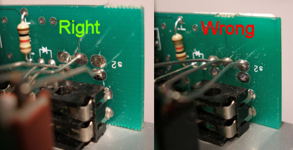
Further down is a plot showing a family of envelopes having swapped out this resistor. (When I first saw this I thought that maybe it was a build-error in my module, but since then I have seen or heard of about half-a-dozen other modules (both MkI and MkII) which have the 6k8 value, so it was either a rather poor design choice, or possibly just a simple mistake.) Contour switch wiring. Presumably due to some perceived difficulty in working out beforehand which way the contour switch needs wiring in order to give log envelopes one way, and exponential ones the other, two sets of holes allowing the connections to be crossed-over were placed on the PCB. Unfortunately the simple act of allowing connections to be made both ways means that sooner or later modules will be built with the connections in the wrong set of holes. OK, so this is hardly a show-stopping problem, but if you like things to be done properly/to be the right way round, then this photo shows how the switch should be wired in order to give log envelopes when it is up, and exponential ones when it is down:
The bottom two traces in the following (rather busy) plot show the log and exp envelopes; the top traces show the linear envelope after having swapped-out the 6k8 resistor for a 10k (see above):
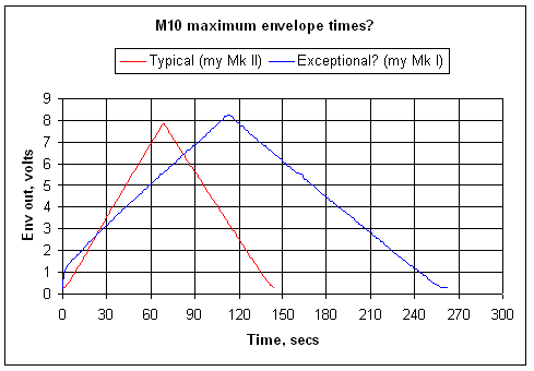
Maximum envelope times: The M10 module description page at the Plan B/EAR website suggests that envelope times of 20 minutes and over are possible, but from modules I've actually measured, such claims are wildly optimistic—a typical maximum envelope time is probably around two and a half minutes, i.e. 150 seconds. The limiting factor is the input bias current of the LM3900 amplifier section of the main integrator driving capacitor C3, which I assume has a standard fitment value of 470nF. The following plot shows the maximum envelopes from both my MkII (at 144 secs), which looks to be typical, and my MkI, which looks to be an exception (263 secs):
(The plots are with both 'rise' and 'fall' pots fully clockwise; Thus the two most obvious possibilities for increasing the max envelope times are to either replace capacitor C3 with a larger value, or specifically select an LM3900 chip (for U3) which gives a longer-than-normal time. [Here are the simple calculations which back up the approx 150-second maximum envelope time assertion. With the rise and fall pots fully clockwise, there is no contribution from either to speed-up the charging of the main integrator cap C3—the only current having an effect is the input bias current, which is given a typical value of 30nA on the TI LM3900 datasheet. It stays constant, so we can use it simply in the familiar relation of I=C dv/dt for a capacitor; C is 470nF, and we want the time for the integrator to reach approx 4.9V, which marks the end of the rise phase, and then multiply by two, to allow for the fall phase too (the 4.9V level is seen as the kink in the 'ramp' output, which is the main integrator output, when rise rate ≠ fall rate). Thus rearranging, we want tmax =2×C×V/I =2×470n×4.9/30n =154 secs.] [Page last updated: 06 Dec 2015] |
||||||||||||